With our Custom Packaging Services, you can get your parts exactly the way you want them without having to outsource to another provider.
There may be cases, for instance, where you want the functionality that a standard part offers, but it just doesn’t fit your application properly. Simply tell us what you need and our engineering team will design the part so that it fits your application. Here are some of our capabilites:
If your application or program demands a smaller, more reliable packaged component, All Tech can deliver a one source solution with our chip scale packaging. Chip scale packages offer near-die size footprints and reductions to package thickness and weight.
A chip scale package combines the performance and size advantages of flip chip bare die and the reliability of an encapsulated device in one tiny package. Chip scale packaging is the ideal solution for battery-powered small form factor devices such as industrial sensors and a variety of defense applications.
We offer a wide array of flip chip assembly capabilities, from single chip placements to multi-chip module and system-in-package assembly of multiple die and components.
With our partner, Micross, All Tech offers access to a 2.5D/3D technology platform through joint development projects, prototyping services and small volume production. The 2.5D/3D integration technology platform is based on several enabling process modules, which include:
Providing full assembly services as well as the one source for all of your packaging needs.
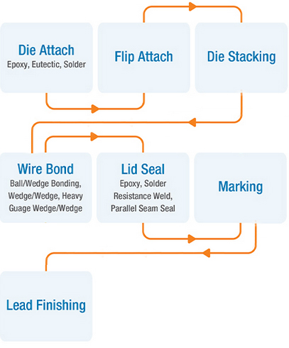
Unlike many of our competitors, we have a comprehensive array of assembly capabilities. Our automated and state-of-the-art die attach, wire bond, encapsulation and CSP capabilities allow us to provide competitive solutions for a broad range of technologies. In addition, manufacturing sites are registered to the AS9100 Standard reinforcing our commitment to always providing the highest quality of products and services while continuing to meet the stringent needs of our aerospace, space, defense and medical customers.
![]()